Indian semiconductor ecosystem: News, Updates & Discussions.

 
That fab in IISc, they demanded 3000 crore, they got 300 crore.
is that maybe the in initial investment while the rest may come later?

sure But India has a stated ambition for lower nm nodes. Tata and PSMC have alr sent a proposal to the gov to upgrade the current fab being built to go down to 14nm.

Whether the stated ambition transitions to reality is yet to be seen but clear steps are being taken for this to happen. You have partnerships with IMEC and IBM and now ASML(although this is more for the machines in the current fab). Lets see. We will know approx 5ish years from now ig.
Hope we also start manufacturing ram's, processors and fast storages because the current market price is way too high for these components.

So no ATMP facility currently?
 
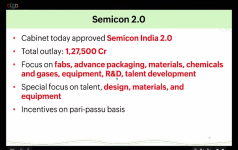
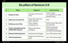
ehhh i was hoping for a 20B+ fund but I guess the electronics fund got the extra 40k cr by using taking away some money from this fund. i do hope this brings in proper large scale display fabs though so that we can finally source fully domestic displays for mobiles and what not.
 
ehhh i was hoping for a 20B+ fund but I guess the electronics fund got the extra 40k cr by using taking away some money from this fund. i do hope this brings in proper large scale display fabs though so that we can finally source fully domestic displays for mobiles and what not.
 
  • Informative
  • Like
Reactions: Shan and spice
Dixon Technologies in talks to set up $3 billion display fab unit in India

Noida-based contract electronics maker Dixon Technologies is in discussions with a global technology company to set up a display fabrication (fab) unit in the country entailing an investment of nearly $3 billion, said its managing director Atul Lall.

The company is also in final discussions with a large overseas original design manufacturer to establish a joint venture for expanding into high-end product categories such as notebooks, servers and IT products, he said.

"We are in active discussion with a global technology partner for setting up a world-class display fab. Currently, India relies heavily on the import of displays. A foray into the segment will aim to localise production and bring greater control over the supply chain and cost efficiencies," Lall said on an earnings call with analysts late Monday, after the company announced its third-quarter results.

"We are awaiting the rollout of policy guidelines under ISM (India Semiconductor Mission) 2.0 by the government of India to take this project forward. This will significantly enhance our value addition," he said.

"A large part of that capex should be subsidised by the government. Our share of capex contribution should be lower, but the overall capex requirement for a display tab is around $3 billion." Under the earlier ISM guidelines, the Centre offered a 50% capital subsidy on pari passu (equal footing), while certain state governments offered 20% on pari passu.

"It is an extremely attractive project with hugely margin accretive and a very fast payback period," Lall said.
 
  • Like
Reactions: BoredBear and spice
is that maybe the in initial investment while the rest may come later?


Hope we also start manufacturing ram's, processors and fast storages because the current market price is way too high for these components.


So no ATMP facility currently?
Yea idt you quite understand how brutal the memory market is and how difficult it is to manufacture memory chips (NAND and DRAM).

India will start (read start lol) to build a fab for that no less than 10-15 years from now.

TSMC doesn't even make memory chips and Intel which invented DRAM literally was pushed out of the market. So I will leave it at that in explaining how brutal memory chip production is.
I will lose my mind if we get a semi-conductor fab equipment startup from a college hackathon:


Bro what. Semiconductor manufacturing equipment for even say 28 nm is literally as hard to make as a 120 kN turbo fan! A country like China has not even fully mastered such equipment even for 28 nm technology which appeared decades ago, they are still reliant on ASML for even that old node.

As for EUV, its harder to make EUV than even military turbofans 💀💀💀. Theres a reason why only 1 company in the entire world can manufacture that in scale.
 
  • Like
Reactions: spice
In chip design Indian talent is superb and world leading. But nobody is talking about the actual EDA tools which are used to develop chips. Only 3 such tools are there from Synopsis, Cadence and Siemens and all 3 are from the West with 2 of them from the US. No alternative as of yet exists. Without these tools it is IMPOSSIBLE to design any chip no matter how advanced it is.

Now India must focus on building a domestic alternative. Basically the main challenge is mapping the RTL code to the hardware implementation: how to efficiently take logic code and netlist and then produce the equivalent pattern of the billions and billions of transistors which implements them, these are done via advanced algorithms developed by Cadence and Synposis.

Idk about Cadence but my friends dad works for Synopsis and says his office in the US is basically 70% Indian engineers. So India needs a coherent strategy for a domestic EDA tool using tapped talent from those companies. Otherwise even if we master semiconductor production of planar technology (don't expect FinFet level for next decade), it will be useless if somehow our access to such tools are pulled and we can't even design chips in the first place
 
  • Like
Reactions: Shan and spice
@Gautam Could tata perhaps partner wit intel for their advanced nodes like intel 3 or intel 18a, intel seems pretty eager to expand their IFS and Tata has the money to do this while India has both the current and future demand.
You want Intel to give 18a to India? Ask Lawrence Livermore Labratory for transfer of W87 warhead while you're at it 🤣. Or Pratt and Whitney to transfer F135 technology to India.

The latter is more likely than Intel giving 18a and both are less than atomic diameter number distance from 0.

Didn't expect such a silly comment from you tbh.

First read about how advanced 2nm level production is and what intel had to go through go achieve that, and the supporting infrastructure, cost and ecosystem it takes to reach that level before daydreaming sir.
 
sure But India has a stated ambition for lower nm nodes. Tata and PSMC have alr sent a proposal to the gov to upgrade the current fab being built to go down to 14nm.

Whether the stated ambition transitions to reality is yet to be seen but clear steps are being taken for this to happen. You have partnerships with IMEC and IBM and now ASML(although this is more for the machines in the current fab). Lets see. We will know approx 5ish years from now ig.
Expect a decent yield (maybe like 93% or something) of 28 nm and high yield of larger nodes. No possibility of FinFet (14/16 nm class and below). In anyways this nm thing is a marketing tool which actually denotes the chips level of performance than actually the size of the transistor.

Nontheless it will India decade at least to reach high yield of 14 nm class chips maybe less with extensive foreign know how transfer. Even longer to go below 10 nm class performance chips.
 
Does ISM2 contain provisions for supporting rad hardened chip manufacturing for low volume applications in mil & space?
We already do that via Shakti for ISRO (RCI DRDO probably used them too) but they are made using old 180 nm technology.

Using advanced nodes for space and rockets are non ideal because there are higher non idealities such as diffusion of electrons between the source and drain of the MOSFETS and quantum switching of electrons between the gate and channel. For space 65 nm and above is ideal.
 
  • Like
Reactions: jmaxwell_