Indian semiconductor ecosystem: News, Updates & Discussions.

Rajasthan-based Sahasra Semiconductor will start the commercial production of first Made in India memory chips from September or early October . company has set up its semiconductor assembly, test and packaging unit in Bhiwadi district from where it will initially package basic memory products like MicroSD cards, chip-on-board, etc and will later move on to advanced packaging of products such as internal memory chips.


Unlike Micron that produces its own chips, Sahasra is more an Outsourced Semiconductor Assembly and Test (OSAT) company, which means they assemble and package chips for other brands.
 
Control and Readout System for Quantum Processor

1694621366071.png


Quantum computers can solve certain computational problems much faster than ordinary computers by using specific quantum properties. The basic building blocks of such machines are called quantum-bits or qubits. Qubits can be realised using several physical platforms such as nuclear spins, trapped ions, cold atoms, photons, and using superconducting Josephson circuits. Several such qubits operate in the microwave frequency domain, and require specialised room temperature microwave electronics for control and readout of the quantum states of the qubits.

However, there lies a challenge when it comes to connecting classical electronics to these qubits. The qubits need high frequency (GHz) electromagnetic signals for control and readout pulses in the order of a few tens of nanoseconds. The traditional setup for generation and capture of such signals is often costly and complex with many components. This can be addressed by developing a specific FPGA-based system that brings the functionality of all the traditional equipment on to a single board. However, with such developments, three main challenges need to be kept in mind: generation and capture of the high-fidelity microwave signals, scalability, a user-friendly interface.

In a new study, researchers from the Departments of Physics and Electronic Systems Engineering, IISc, have addressed these challenges with the development of Scalable Quantum Control and Readout System (SQ-CARS), using Xilinx RFSoC FPGA board. The team tested their SQ-CARS system by conducting different experiments with superconducting transmon qubits and benchmarked it against the traditional setup.

“SQ-CARS is quite a versatile electronics platform which has been extensively tuned up for speed, scale, complexity and cost, while measuring multi-qubit devices in the microwave domain,” says Vibhor Singh, Associate Professor in the Department of Physics, IISc, and one of the authors. “To the best of my knowledge, it is the first of its kind deep-tech effort from India.”

With SQ-CARS, the researchers have developed a scalable and user-friendly platform for physicists to carry out advanced quantum experiments at a fractional cost (more than 10x reduction in the cost) and huge reduction in terms of size.

“The core challenge in practical quantum computer development is integrating a large number of qubits with control and readout electronics. This work lays the foundation for scalable indigenous quantum processors,” says Chetan Singh Thakur, Associate Professor in the Department of Electronic Systems Engineering, IISc, one of the authors.

1694621404839.png


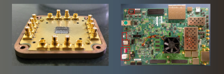
Top left: Image of the electronics rack showing various test and measurement equipment used in the experiments. Top centre: Photo of the superconducting chip along with its packaging. Top right: Photo of the developed boards running SQ-CARS. Bottom right: Mounting of the qubit chip in the low temperature setup. Bottom left: The complete measurement setup showing the picture of the dilution refrigerator which operates at 10 mK.
1694621441014.png


Research paper: SQ-CARS: A Scalable Quantum Control and Readout System

Source: Indian Institute of Science
 
  • Like
Reactions: Ashwin
This Engineer Is Helping to Make India a Global Semiconductor Hub

He is leading the development of next-generation chips

KATHY PRETZ
24 SEP 2023
1696241598574.png

Tushar Sharma
joined Renesas Electronics executive vice president Sailesh Chittipeddi [far left] and the company’s CEO Hidetoshi Shibata in presenting India’s Prime Minister Narendra Modi with a framed 5G chipset. Photo: PRIME MINISTER OF INDIA OFFICE


When Tushar Sharma was a young boy growing up in Jamnapaar, India, a densely populated area outside of Delhi, he never imagined that someday he would meet the country’s prime minister.

That memorable event occurred in May, when Sharma and a delegation from his employer, Renesas Electronics, met with Narendra Modi to discuss how the semiconductor company could support the prime minister’s India Semiconductor Mission and Digital India initiative. The initiative aims to improve the country’s reliance on hardware infrastructure and to become a global hub for electronics manufacturing and design.

Sharma, a semiconductor engineer, was instrumental in organizing the meeting for the Tokyo-based company. He heads the recently opened Renesas-Tata Consultancy Services Joint Innovation Center, in Bengaluru. The center focuses on radio-frequency, digital, and mixed-signal design, as well as software for next-generation chips focusing on 5G, artificial intelligence, the Internet of Things, and more.

Renesas’s efforts for the “Made in India” ecosystem reflects the company’s expertise in manufacturing, telecommunications, automotive, and advanced semiconductor design, Sharma says.

“The idea is to enable more end-to-end solutions for India as well as other global markets,” he says. “India has to become a self-sustaining R&D hub.”

Building a thriving semiconductor industry

At the meeting with Modi, Sharma presented the prime minister with a cutting-edge 5G millimeter-wave and sub-6-gigahertz chipset designed by Renesas’s R&D teams in Bengaluru and San Diego.

“The prime minister displayed a genuine fascination with the chipset and talked about the technical intricacies of the integrated chip,” the IEEE member says. “He asked about the silicon node and the fabrication facility that created it."

“I firmly believe the development of these critical chips is vital for the greater public good,” Sharma says. “Those working in industry can be change agents and have a meaningful impact on society, such as advancing technology for humanity. After all, that is the motto of IEEE.”

Sharma worked for several years as an RF engineer in the semiconductor industry before joining Renesas in 2021. He is based at the company’s San Diego office but travels frequently to Bengaluru. Sharma’s research includes developing gallium nitride technology, advanced integrated circuits for 5G and beyond, and millimeter-wave transmitters.

In addition to leading the innovation center, he is a visiting professor at the Indian Institute of Technology Bombay and advisor to the university’s Center for Semiconductor Technologies. The SemiX focuses on workforce development and entrepreneurship by serving as a common interdisciplinary platform between academia, industry, investors, and government. The center supports the Indian Semiconductor Mission, which aims to grow the nation’s chip industry.

When Sharma asked the prime minister to share his vision for India’s future, Modi told him it was important that young professionals and those working in the scientific community be involved in fostering inclusive growth, developing talent, and improving the skills of those living in the country’s rural areas, focusing on technology development with integrity, inclusion, and innovation.

Sharma says he finds Modi’s own career inspirational, because he experienced the challenges of growing up in a financially strained environment.

“His tech-savvy approach—and active presence on social media with more than 200 million followers—allows him to connect and engage with the youth, addressing their concerns and aspirations in a relatable manner,” he says. “What resonates with young professionals is the belief that no dream is too big, and no obstacle is too insurmountable when fueled by a strong sense of purpose and a vision for a brighter future.”

From astrophysicist to semiconductor engineer

Growing up in a financially strained environment, Sharma joined the Society of Amateur Radio Astronomers, seeking mentorship and support from nearby science clubs. He learned how to set up antennas and radios to track celestial events.

He wanted to monitor and record the radio waves from the annular solar eclipse in 2013, but he couldn’t afford a radio, so he decided to build his own. He bartered with shop owners to get free parts in exchange for tutoring their children.

While building his radio, he says, he fell in love with engineering.

“I went through so much emotion and hard work that I got attracted to the engineering field,” he says. “I realized that engineering is the backbone of many things that are used in our daily lives.”

To get to the best place for him to view the eclipse—Varkala, Kerala, which is 2,500 kilometers from his hometown—he took buses and trains, and he walked at times. At the viewing site, he met solar physicist Subramaniam Ananthakrishnan. After Sharma showed him the radio he had built, Ananthakrishnan encouraged him to pursue a career as a semiconductor engineer and challenged him to design an amplifier that did not oscillate and an oscillator that didn’t amplify. Sharma did just that.

“Those working in industry can be change agents and have a meaningful impact on society.”

He earned a bachelor’s degree in engineering in 2009 from Guru Gobind Singh Indraprastha University, in Delhi. He wanted to continue his studies in the United States, he says, but the tuition was too expensive.

By chance, he attended a session on microwaves given by IEEE Fellow Fadhel Ghannouchi, who taught electrical and computer engineering at the University of Calgary, in Alberta, Canada. Sharma told Ghannouchi about his research and his work with radio waves. Ghannouchi encouraged him to apply for a Killam Doctoral Scholarship to the Canadian university, and he was accepted. Sharma earned a Ph.D. in electrical and computer engineering in 2018 from the university, followed by a postdoc stint at Princeton. Calgary recognized him with a Schulich Early Achievement Alumni Award in 2019.

An active student humanitarian

Since his college days, Sharma has been using his technical skills to give back to communities around the world. He started as an IEEE student branch chair. His focus, he says, has been to encourage students to pursue a STEM education and to bridge the digital/education divide.

When he moved to Canada, he joined the IEEE Southern Alberta Section and served as chair of its Young Professionals affinity group. He helped reinvigorate the group, which received the 2015 Young Professionals Hall of Fame Award. The honor recognizes groups that have formed collaborations with local industry, organized quality events, engaged with other IEEE units, and held activities that grew their membership.

Sharma helped found the section’s IEEE Special Interest Group on Humanitarian Technology. The SIGHT group partners with local organizations to bring technology to underserved communities. Looking for people who needed help, he learned about the indigenous community in Canada.

“I was shocked to see that within first-world countries, there is still so much disparity,” he says.

The IEEE SIGHT group built the infrastructure to bring free Wi-Fi to the Maskwacis reserve, in central Alberta. The project received US $20,000 from what is now the IEEE Humanitarian Technologies Board.

“I understood one thing: that it’s not always about the solutions; it’s about working on the right problems,” Sharma says of his SIGHT work.

“Wireless connectivity is a basic need for individuals because that’s what connects them to the outside world and the global ecosystem,” he says. Thanks to the project, he says, residents could start small businesses and sell their products online.

“Technology is not just about high-end IC design,” he says. “It is also about how you can translate that technology into public good.”

In 2021 Sharma was the youngest member to be elected to the IEEE Microwave Theory and Technology Society board, on which he still serves. He says he values getting to meet the other board members, who include some of the best researchers in their field who are shaping the future of technology

What’s more, he says, “I get to evolve my personality, understand how technology trends are changing, and what the strategies are.

“For my professional career, membership has helped me expand my network and sharpen my technical know-how. Be it your personal or professional life, learning and service is an inevitable process. The more you serve, the more you learn and grow.”

This Engineer Is Helping to Make India a Global Semiconductor Hub
 
Designed-in-India chips for the World

RISC-V open-source architecture for making chips is spawning a new chip design startup ecosystem in India, including ventures like Mindgrove Technologies

BY HARICHANDAN ARAKALI,
PUBLISHED: Oct 17, 2023 11:57:31 AM IST
1697650317599.png

RISC-V (Reduced Instruction Set Computer-V), pronounced risk-five' started out as a research project at the University of California, Berkeley, around 2010.

Today, it’s a popular, globally adopted open-source instruction set architecture, as computer scientists and engineers call these rules that interface software and hardware.

RISC-V is helping to lower the barriers of entry erected by companies that have amassed proprietary chip design IP (intellectual property) that they licence—only the world’s biggest tech companies can afford that, and even they are investing heavily in building their own chips. Apple Silicon is perhaps the best-known example.

And the iPhone maker’s recent extension of a deal to continue to buy 5G modems from Qualcomm, shows how difficult it is to develop a chip from scratch—even a trillion-dollar company hasn’t cracked the modems yet. This is why efforts like RISC-V are a godsend for India.

1697650361587.png


A nascent RISC-V ecosystem is coming up in India comprising engineering teams such as those led by professor V Kamakoti at IIT-Madras, father of the Shakti microprocessors, startups such as Mindgrove Technologies that are developing commercial systems-on-chip (SoC), based on Shakti core, and VC (venture capital) firms such as Speciale Invest and Peak XV Partners who are backing such startups with seed money.

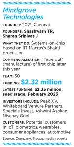
Shashwath TR and Sharan Srinivas Jagathrakshakan started Mindgrove, incubated at IIT-Madras, to build their SoCs for applications in IoT (Internet of Things), computer vision and automotive sectors.

“Our first chip is targeted for devices like biometric systems, consumer appliances and other embedded use cases,” Jagathrakshakan says.

And “we are currently in the end stages of getting our first prototype out”, Shashwath adds.

“Tape out”, which is semiconductor industry jargon for making the physical chip, could be out as early as November. If all goes well, that chip should be ready to go into a circuit board and it should just work.

If there are flaws, it could be as bad as going back to the drawing board. The duo is developing two more SoCs.

1697650399763.png


“The clamour for chips designed for India, by India is growing every day, and Mindgrove could become an important company in an inevitable market trend towards sovereignty in chip design,” Peak XV’s Anandamoy Rowchowdhary, Vedant Trivedi and Sidhant Goyal wrote in a blog post in May, briefly discussing their “thesis” as VC investors like to say.

In June, Mindgrove also announced a partnership with Imagination Technologies, a UK-based semiconductor design licensing company.

Under the partnership, Mindgrove will get access to IP owned by Imagination that will help Mindgrove build its own graphics processors and artificial intelligence accelerators.”

Designed-in-India Chips For The World - Forbes India
 
India working towards development of Silicon Photonic Processor Chips. MeitY inaugurated the Centre for Programmable Photonic Integrated Circuit & Systems at IIT Madras. India is actively fostering the development of diverse PIC tech platforms, including silicon photonics, diamond photonics, polymer photonics,& lithium niobate photonics. Within the next 5 years, CPPICS is set to achieve self-sufficiency, drive product commercialization through startups, &provide essential training to bolster the future ecosystem of PIC manufacturing in India.
1697983025336.png


  • Like
Reactions: GOW
Semiconductor Laboratory revamp: Tata, Texas, Tower among nine bidders

By Aashish Aryan & Surabhi Agarwal, ETtech
Last Updated: Jan 31, 2024, 06:00:00 AM IST

Synopsis
The state-owned Semiconductor Laboratory in Mohali is the only chip manufacturing unit in India that produces semiconductors for strategic and defence purposes, including for space exploration such as the Chandrayaan mission. However, the facility that was founded in 1976, has lagged behind private companies in terms of production as well as technology over the years.

1706719627282.png

The Semiconductor Laboratory (SCL) in Mohali.

The government has received nine bids, from companies including the Tata Group, Tower Semiconductor and Texas Instruments, for the overhaul of its Semiconductor Laboratory (SCL) in Mohali, said people with knowledge of the development.

The government has earmarked about $1 billion for the modernization of the 48-year-old facility.

The state-owned plant is the only chip manufacturing unit in India which produces semiconductors for strategic and defence purposes, including for space exploration such as the Chandrayaan mission. “The need for modernization of SCL is for a strategic purpose,” a senior government official said, adding that it is keen that a local firm gets the mandate since a lot of the work is of national importance.

The Tata Group has been preparing to enter the chip manufacturing segment in India for the past few years. Its chairman N Chandrasekaran said earlier this month that it will set up a chip manufacturing unit at Dholera soon.

Israel’s Tower Semiconductor has a close association with SCL as it had helped the Indian government plan the 180 nanometers chip plant. Tower Semiconductor is also very keen to enter the commercial chip manufacturing segment in India and has been in active discussions with the government while Texas Instruments has significant chip research and development operations in the country.

“Once the government decides on the exact nodes that the facility will manufacture, financial bids will be invited from these companies,” said another senior government official. The firm, which will be given the final mandate, may have to partner with a technology firm that has licensing grade semiconductor technology, the official added.

1706719487161.png


The Tata Group, Tower Semiconductor and Texas Instruments did not respond to ET’s queries till press time.

At present, the government-run Mohali facility produces chips of 180 nm node size, which have very limited use cases. The ministry of electronics and information technology (MeitY) officials said the goal is to bring the technology of the facility on a par with industry standards of legacy nodes of 65 and 40 nm to start with, before aiming for more cutting-edge nodes.

Founded in 1976, as Semiconductor Complex Limited, the organization was meant to further India’s ambitions of semiconductor manufacturing. The facility has, however, lagged behind private companies in terms of production as well as technology over the years.

The government therefore earmarked $1 billion for modernization of the facility and invited expressions of interest from the industry in September last year. The $1 billion fund is part of the government’s $10 billion semiconductor incentive package to set up a semiconductor chip fabrication ecosystem in the country.

“We are hopeful of getting more bids, especially from domestic companies since a lot of the work is of crucial national importance. We are evaluating the current bids including from the Tata Group. A couple of companies working in the defence space have also shown interest,” said one of the officials cited earlier.

SCL does not need to get into the commercial production of chips, the official said, adding, “It has been doing continuous research and development (R&D) work in the past and will continue doing so.”

Satya Gupta, the chief executive of Epic Foundation, a semiconductor-focused not-for-profit advocacy group, however said SCL would benefit by having some commercial focus.

The government will also need to set “definite” commercial and strategic goals for SCL, especially in terms of the revenue the facility can generate commercially, he said.

“Ideally SCL should plan for $50 million revenue in five years, 80% of which should come from commercial operations including skilling and 20% from products for the strategic sector. Based on these goals and product mix, adequate technology, infrastructure and talent should be planned and created,” Gupta said.

In September 2023, the electronics and IT ministry had invited bids for modernisation of the Mohali facility either by transforming it into a research and development centre of excellence or an at-scale manufacturing facility or a combination of both.

In its bid document, the ministry had then said that SCL would continue to fulfil the semiconductor chip demand of government agencies such as the Indian Space Research Organisation.

The ministry had also mandated that the bidder would need to ensure end-to-end set-up and operationalisation of the R&D fab and look at technology transfer, material and equipment supplies, installation, operational testing, commissioning, onsite and offsite skilling of operational manpower and periodic maintenance.

Semiconductor Laboratory revamp: Tata, Texas, Tower among nine bidders
 
  • Like
Reactions: Ironhide
Analog Devices to Make Custom Chips for India

The company is also open to the prospect of testing and packaging some of these chips in India.

by Pritam Bordoloi
Last updated February 6, 2024
1707241270515.png


A global semiconductor leader, Analog Devices, last year recorded $12.3 billion in revenue. Even though the contribution from India towards its global revenue share is minimal, India is emerging as one of the fastest-growing markets for Analog. Besides, the US-based semiconductor company also has plans to develop chips locally.

“We are particularly interested in the industrial market, given India’s emergence as a manufacturing hub. The shift towards smart factories is evident, and Analog, with a robust portfolio in industrial and process automation, plays a significant role,” Srinivas Prasad, senior director and site head at Analog Devices India (ADI), told AIM during an interaction on the sidelines of the IESA Vision Summit 2024.

Vivek Tyagi, managing director-field sales at ADI, concurs. He believes that the Indian market will definitely explode in the next seven to eight years. “So, we expect significant growth accordingly, even though this year is a little soft globally, we are still forecasting a 20% growth in India from our sales,” he told AIM.

In fact, Analog Devices anticipates India’s contribution to global revenue share to increase multifolds by 2030. The growth forecast is a result of India’s renewed focus on manufacturing.

In the recent Union budget, the government allocated INR 15,500 crore for various electronics manufacturing programmes, including the semiconductor mission and mobile and IT hardware PLI schemes for FY25.

En Route to India

Analog Devices, headquartered in Wilmington, Massachusetts, operates an R&D centre in India. The company serves around 100,000 customers across various industries, including communications, computer, instrumentation, military, aerospace, automotive, and consumer electronics applications.

Even though the company has an R&D centre on almost all continents, each chip that undergoes tape-out proudly bears the contribution of the Indian team. “We anticipate this trend to continue, with more innovations, products, and strategic solutions emerging from India. Today, I can confidently affirm that every chip undergoing tape-out has involved the expertise of our Indian team,” Prasad added.

Moreover, given India is one of Analog Devices’ fastest-growing markets, the company is considering building some chips in India to cater to the Indian market.

However, Analog Devices has no plans to fabricate its chips in India. “The crucial aspect is the design, which is paramount because it involves gathering precise specifications from the customer, and having the design team in India ensures the creation of the right chip that can then proceed to manufacturing,” Tyagi said.

Nonetheless, given so many Outsourced Semiconductor Assembly and Test (OSAT) units are coming out of India, he won’t write off the fact that the company could test and package some of its Indian chips locally.

Unleashing Innovations

Semiconductor companies envision not only potential revenue growth but also innovation within the automobile industry. As the sector shifts towards electric, hybrid electric, and autonomous vehicles, the demand for semiconductors sees a significant surge.

Analog Devices has also unveiled innovations in battery management systems (BMS), cockpit solutions, and advanced driver assistance systems (ADAS) aimed at assisting the automotive sector in transitioning towards a more software-defined vehicle.

In India, the company is taking its innovation to both two and four-wheeler original equipment manufacturers (OEMs) in the country.

“For EVs, their reliance on batteries as the primary source of fuel underscores the critical importance of battery management. Analog Technology, an expertise of Analog Devices, plays a pivotal role in this domain. Analog Devices holds a commanding position, accounting for over 50% of the global market share in battery management solutions for cars, solidifying a robust presence, particularly in India,” Tyagi said.

Moreover, Analog Devices’ automobile-focussed innovation also revolves around enhancing the cabin experience. From multimedia and telematics to improved battery performance, the shift to EVs brings a demand for differentiated experiences.

“As this transition unfolds, consumers, especially in India, are increasingly seeking a differentiated experience in their cabin environment. This extends to advanced infotainment systems, improved air conditioning, a desire for a comprehensive surround experience, and advancements in camera technology,” Prasad said.

Analog Devices offers a range of camera solutions for ADAS, powered by their semiconductor chip. These are complete automotive grade solutions powered by GMSL2 (Gigabit Multimedia Serial Link) interface.

“The focus is also on developing capabilities for vehicle-to-vehicle communication channels. While certain features may necessitate sophisticated infrastructure, there is a growing willingness among consumers to invest in enhanced automotive experiences,” Prasad added.

Invests heavily in AI

For Analog Devices, AI is also a big focus area and the semiconductor company has developed AI chips, according to Prasad. The company is also closely monitoring emerging trends and reimagining conventional approaches using AI.

“I believe every segment, from sensors to the cloud, will be influenced by AI. This is also our trajectory,” he said. However, at the same time, it’s also crucial to discern which applications are truly beneficial, avoiding unnecessary additions.

Analog Devices asserts that its focus is on pioneering intelligent edge solutions with smart, efficient algorithms. While conventional algorithms served a purpose, AI is now enhancing them for greater accuracy and efficiency.

“In sectors like vision sensing in automotive and robotics, our focus is on crucial factors like collision detection and providing a comprehensive 360-degree view for informed edge decisions. Analog Devices is actively advancing AI-based solutions in these areas,” he said.

Generative AI Experiments

Today, we are in the era of generative AI and companies across diverse industries are actively exploring various use cases for this transformative technology.

Many aspects of these technologies are still evolving. Prasad feels creating countless use cases is essential for practicality, especially in scenarios where false positives can have severe consequences, such as healthcare.

Currently, Analog Devices is testing generative AI internally in areas of manufacturing and chip designing. “We focus on non-critical applications, as the technology is still in the early stages, with everyone engaged in their research and development phase. Commercialisation benefits will take time to materialise,” he concluded.

Analog Devices to Make Custom Chips for India
 
[Exclusive] Mindgrove Technologies’ Shashwath TR on Making India’s Most Secure Chip
Mindgrove Technologies is currently working on its inaugural chip Secure IoT designed for a range of consumer electronics.

by Siddharth Jindal
Last updated January 31, 2024

1707241490297.png

The Indian IT Minister Rajeev Chandrashekhar recently lauded Mindgrove Technologies for building globally competitive next gen devices/products, and its contribution to India’s ever evolving semiconductor landscape.

“It’s really encouraging coming from someone who actually understands the industry and follows us very closely,” said CEO and founder of Mindgrove Technologies, Shashwath TR, in an exclusive interaction with AIM. He also shared his recent conversation with Prof V Kamakoti (the brain behind Shakthi microprocessor) and said: “This is the first time in my life I’ve gone to a meeting with a politician and talked about how the processor works.”

Founded in 2021, Mindgrove Technologies is a Chennai based semiconductor company focusing on the design and production of Systems on Chips (SoCs). Mindgrove has used the Shakti core as the foundation for their SoCs. Shakti is an open-source RISC-V processor core developed by the Indian Institute of Technology Madras (IIT-M), and backed by MeitY.

The fabless startup secured $2.32 million in seed funding last year from investors led by Sequoia Capital India (now Peak XV Partners). It told AIM that it looks to raise more funds from the Indian Government and other investors for the upcoming projects. Shashwath said that it plans to raise money in its Series A round for product enhancements and business expansion.

Mindgrove Technologies’ Chips

Shashwath’s company Mindgrove Technologies is currently working on its inaugural chip Secure IoT designed for a range of consumer electronics, such as TVs, washing machines, air conditioners, refrigerators, and other devices. This multi-processor chip comes with security accelerators, true random number generator, and one-time programmable memory.

Mindgrove Technologies said that it has successfully reached the prototype production stage. In the coming months, it looks to launch the prototype.

Secure IoT’s production is based on MPW (Multi-Project Wafer). This enables cost-effective prototyping and low-volume production, reducing the cost of a full prototyping wafer run to 10% or even 5% of the initial price.

“Typically, during production, the entire wafer is dedicated to one chip. But on a multi-project wafer (MPW), you get 100 chips on that wafer,” said Shashwath, saying that the company is currently waiting on the packaging. “The packaging is going to take a little longer. And once that is ready, we can put it on a board and test it,” he added.

Shashwath said that the chip would be ready early next year for shipping. “Q3 and Q4 of 2024 is when we can actually start placing volume orders with the foundry. Then, with roughly three months of lead time, by Q4 of 2024 or Q1 of 2025, we can actually start shipping the chips in large volumes,” explained Shashwath.

He further said this has helped them reduce the cost significantly. “We are 50-60% cheaper at the top end of the market,” said Shaswath, saying that they are a little more expensive at the bottom end of the market, but would be of higher quality when compared to subpar or third-grade chips.

What’s next?

Shashwath said that the next line of products includes Vision SoC and Edge Compute, which will focus on the automotive industry (vehicle infotainment) and edge computing for AI inference, respectively. The Vision SoC is going to be quad-core. “My target is to get a prototype out early next year,” said Shashwath.

“A lot of people in the industry — customers, suppliers, partners, government, all of them — needed to take us seriously. That was probably the biggest challenge that I faced,” he said, noting that many of those who were initially skeptical are now good friends.

“We don’t build chips for the sake of building chips. We are building chips to solve problems” concluded Shashwath.

[Exclusive] Mindgrove Technologies’ Shashwath TR on Making India's Most Secure Chip
 
  • Like
Reactions: HariPrasad
The SHAKTI-Man of India

Professor Kamakoti built SHAKTI, which is India's first open microprocessor on top of the open RISC-V architecture and is funded by the MeitY.

by Mohit Pandey
Last updated February 6, 2024
1707241798383.png


The SHAKTI-man of India, Veezhinathan Kamakoti, the director of IIT Madras, has had a hectic few years. The genius behind India’s first microprocessor has been trying really hard to build semiconductor capabilities in India, and put a stop on cheap imports from China. “This is something we have achieved over the past 10 years; I have completely given up every other thing to work for SHAKTI,” he told AIM in an exclusive interview.

Kamakoti started building the SHAKTI microprocessor in 2014, an open processor built on top of the open RISC-V architecture, which is funded by the Ministry of Electronics and Information Technology. He said that there is a need for building hardware that supports building AI models within the country, which led him to take the charge with the SHAKTI microprocessor.

For the past few years, Kamakoti has been rallying for an increase in the investments for semiconductor startups, which is still viewed as a risky area for many VCs.

“I am only Saraswati, not Lakshmi for these startups,” Kamakoti said, and informed that there are five companies coming out of the IIT Madras lab: Incore, Mindgrove Technologies, Chakra Electronics, Vyoma Systems, and SecurWeave. All of them are building on top of the SHAKTI core, but he is only the mentor for these companies. “It is very interesting to see that we have an indigenous processor ecosystem in India,” he added.

Building trust for the chip
Since completing his first course in AI in 1992 from IIT Madras, Kamakoti has been finding ways to use AI for social good and solving complex problems within India. This led him to start focusing on hardware and eventually working on SHAKTI, which is also focusing on edge AI use cases.

Kamakoti believes that it is rather difficult to build trust in the semiconductor business because investors need to have full faith when investing in these startups. “Though the government is providing full support for improving the semiconductor industry in India, investors are still hasty and cautious when it comes to investing, as it is a very costly affair, and cheaper alternatives are always available. We are now closing the gap,” he added.

“Today, Shakti C-class is very stable and we have made multiple chips with it. We are ready to give them to startups as well, which is not a joke,” said Kamakoti highlighting that they are making it open for everyone for democratising processor based SoC (system of chips) design in the country.

“Unlike a software company which has a cloud and is developing a software solution with demos, hardware startups take a lot more trust and investment, which the government is promoting, but we need a lot more VCs to take interest as well,” Kamakoti emphasized.

BharatGPT can be the Copilot for India
Kamakoti was the chairperson of the AI Task Force, which was constituted in 2016 by the Ministry of Commerce and Industry. The AI Task Force report highlighted how AI can be used as an economic transformer for the country. Apart from this, currently he is also a crucial member of the BharatGPT initiative, which was started by IIT Bombay.

Highlighting specialized hardware for every field including IoT, network processing, and computing, Kamakoti said that it is also essential for LLMs to be built and catered for specific domains. He believes that this is where BharatGPT is going to play a crucial role. “The initiative requires validation from experts from every domain, and that is what BharatGPT stands for,” he explained.

Giving examples of training small models for the legal and medical sectors and how they can assist professionals in those field, Kamakoti said that the open source approach of BharatGPT will help it become the Copilot for different domains. “It is not a search engine, but a technology that is doing a lot of NLP, and giving you contextual output”, which he believes would help people approach every field with a lot more confidence.

Reflecting on how there are thousands, if not millions of documents in Indic languages, it is the need of the hour to extract knowledge from them, including historical facts and science. “For example, there is some proof that Newton’s laws were present in our ancient texts at least a 1000 years ago,” and this can benefit the whole of the world.

“LLMs are like faithful kids”
Talking about generalized models like ChatGPT and Bard, Kamakoti said that LLMs are like faithful kids. “If you give them relevant data, they will do exactly what you want them to.” He said that there is a dire need for data scientists and to focus on extracting and gathering information for tokenizing these Indic models.

“This would obviously require a lot of money and compute,” highlighting his love for farming, Kamakoti said that while we are also talking sustainability with AI models, they are also very necessary for helping various sectors such as agriculture. “There is a lot of knowledge hidden in rural India, which needs to be brought out,” he added, highlighting that every field, even within the same domain, requires different amounts of data.

Focusing on the recent funding of INR 110 crore from Sunil Wadhwani to IIT Madras for building a school for AI and data science, Kamakoti recalled that a reporter asked him if the same money could instead be spent on building 10-12 schools in India. To this, he replied, “I can use AI to enhance the capabilities of the teacher. I don’t want to replace the teacher, but augment them, in the end creating a very good Co-pilot.”

The SHAKTI-Man of India
 
  • Like
Reactions: Ashwin
Israeli chipmaker Tower closes in on $8 billion fabrication plant in India.

By Soumyarendra Barik
February 11, 2023, 10:31AM

If Tower’s proposal is accepted by the government, it would be the first semiconductor company with real fabrication pedigree to join India’s $10 billion chip manufacturing scheme and will be a big boost to New Delhi’s chipmaking ambitions.
1707642833078.png

Tower is looking to manufacture 40 & 65 nm semi-conductors in India.

Israel-based chip manufacturing company Tower Semiconductor has submitted its proposal to set up a chip fabrication plant in India worth around $8 billion, The Indian Express has learnt. The government is assessing its pitch and is hoping to clear it before the model code of conduct kicks in ahead of this year’s general elections.

If Tower’s proposal is accepted by the government, it would be the first semiconductor company with real fabrication pedigree to join India’s $10 billion chip manufacturing scheme and will be a big boost to New Delhi’s chipmaking ambitions.

The scheme promises a 50 per cent capital expenditure subsidy to successful applicants – meaning that if Tower’s plant costs $8 billion, the Centre will shell out $4 billion from its kitty. Any state where the chip foundry could be located may give additional benefits to the company. Tower is looking to manufacture 65 nanometre and 40 nanometre chips in India which may be used in a number of sectors, including automotive and wearable electronics.

Minister of State for Electronics and IT Rajeev Chandrasekhar had last October met Tower’s CEO Russel C Ellwanger to discuss its partnership with India in the chip space.

Tower Semiconductor did not respond to a request for comment.

Tower had earlier applied to the scheme to set up a $3 billion plant in Karnataka in partnership with international consortium ISMC. However, the plan got stuck due to the company’s then impending merger with Intel. Last August, Intel cancelled its plan to acquire Tower Semiconductor for $5.4 billion due to regulatory issues.

The planned merger between Intel and Tower, announced in February 2022, passed an antitrust review in the United States and several other geographies. But it ran into a lengthy delay in China, where regulators review mergers of companies that earn a certain amount of revenue in the country.

On Friday, CG Power and Industrial Solutions said it has entered into a joint venture (JV) agreement with Renesas Electronics America and Thailand-based Stars Microelectronics to set up a semiconductor assembly and testing plant in India.

While India has managed to attract big names such as Micron Technology to set up a chip packaging plant in the country, it is yet to clear a proposal to set up a full-fledged fabrication plant.

While securing Micron’s $825 million investment commitment for its packaging plant was a big win for India’s chip ambitions, having a chip foundry would be a big milestone and help draw further investments in the chip space.

A joint venture between Foxconn, best known as the manufacturer of iPhones, and Vedanta to set up a $19.5 billion chip plant came to an abrupt halt last year. Foxconn announced it was pulling out of the joint venture with Vedanta. While government sources maintain the two could apply separately, there has been no movement so far.

There was a third fab proposal by Singapore-based IGSS Venture, but it was not found up to the mark by the advisory committee of the government and is on the back burner, it is learnt.

Israeli chipmaker Tower closes in on $8 billion fabrication plant in India
 
  • Like
Reactions: Parthu and Ashwin
Israeli chipmaker Tower closes in on $8 billion fabrication plant in India.

By Soumyarendra Barik
February 11, 2023, 10:31AM

If Tower’s proposal is accepted by the government, it would be the first semiconductor company with real fabrication pedigree to join India’s $10 billion chip manufacturing scheme and will be a big boost to New Delhi’s chipmaking ambitions.
View attachment 31944
Tower is looking to manufacture 40 & 65 nm semi-conductors in India.

Israel-based chip manufacturing company Tower Semiconductor has submitted its proposal to set up a chip fabrication plant in India worth around $8 billion, The Indian Express has learnt. The government is assessing its pitch and is hoping to clear it before the model code of conduct kicks in ahead of this year’s general elections.

If Tower’s proposal is accepted by the government, it would be the first semiconductor company with real fabrication pedigree to join India’s $10 billion chip manufacturing scheme and will be a big boost to New Delhi’s chipmaking ambitions.

The scheme promises a 50 per cent capital expenditure subsidy to successful applicants – meaning that if Tower’s plant costs $8 billion, the Centre will shell out $4 billion from its kitty. Any state where the chip foundry could be located may give additional benefits to the company. Tower is looking to manufacture 65 nanometre and 40 nanometre chips in India which may be used in a number of sectors, including automotive and wearable electronics.

Minister of State for Electronics and IT Rajeev Chandrasekhar had last October met Tower’s CEO Russel C Ellwanger to discuss its partnership with India in the chip space.

Tower Semiconductor did not respond to a request for comment.

Tower had earlier applied to the scheme to set up a $3 billion plant in Karnataka in partnership with international consortium ISMC. However, the plan got stuck due to the company’s then impending merger with Intel. Last August, Intel cancelled its plan to acquire Tower Semiconductor for $5.4 billion due to regulatory issues.

The planned merger between Intel and Tower, announced in February 2022, passed an antitrust review in the United States and several other geographies. But it ran into a lengthy delay in China, where regulators review mergers of companies that earn a certain amount of revenue in the country.

On Friday, CG Power and Industrial Solutions said it has entered into a joint venture (JV) agreement with Renesas Electronics America and Thailand-based Stars Microelectronics to set up a semiconductor assembly and testing plant in India.

While India has managed to attract big names such as Micron Technology to set up a chip packaging plant in the country, it is yet to clear a proposal to set up a full-fledged fabrication plant.

While securing Micron’s $825 million investment commitment for its packaging plant was a big win for India’s chip ambitions, having a chip foundry would be a big milestone and help draw further investments in the chip space.

A joint venture between Foxconn, best known as the manufacturer of iPhones, and Vedanta to set up a $19.5 billion chip plant came to an abrupt halt last year. Foxconn announced it was pulling out of the joint venture with Vedanta. While government sources maintain the two could apply separately, there has been no movement so far.

There was a third fab proposal by Singapore-based IGSS Venture, but it was not found up to the mark by the advisory committee of the government and is on the back burner, it is learnt.

Israeli chipmaker Tower closes in on $8 billion fabrication plant in India
Ambani bhai should just buy them out. :LOL:
 
It seems we are moving up in the semi-conductor world:


@Ashwin @randomradio @Ginvincible @Parthu et al. you guys should see this.

I had written a post about Si2 Microsystems here in 2020 when they started to get defence contracts. Quoting that here:

Si2 Microsystems is one of the few companies involved in System-in-Package(SIP) manufacturing in India. They cater to aerospace, defence, telecom and some consumer electronics segment. They have ISRO, DRDO, MBDA, BOSCH, GE , IBM, HAL et al. as customers.

They have a certified facility with chip level interconnect & assembly technology involving die bonding, wire bonding, flip-chip, etc. Si2 has packaging capability for : FBGA, micro-BGA, BGA, QFN, WL-CSP (Wafer Level CSP) and Ultra compact packages to international quality standards, including special packages for sensor media access, hermetic packages for military and aerospace. PCB assembly with fine pitch components, WLCSP’s, PoP etc. extending to complete box build.


View attachment 16938
View attachment 16939

They also do contract manufacturing for other processor design companies like Analog Devices & Cosmic Circuits. Cosmic Circuits was an Indian company that designed and licensed IPs for their SoCs. Cosmic was acquired by US based Cadence Design Systems.

Thin Ball Grid Array (TBGA)-500 pin packaged Video processor for Cosmic Circuits :
View attachment 16936

Plastic Ball Grid Array (PBGA)-352 pin processor for Cosmic Circuits :
View attachment 16937

In February 2020, Si2 signed a MoU with BEML for jointly exploring the defence market for electronic, RF and surveillance systems.

These guys make microprocessors for RF & IIR missile seekers, electronic surveillance & jamming equipment. If I remember correctly, the Navy wanted to upgrade the seekers of their Kh-35E cruise missiles. For this upgrade DRDO & pvt. companies worked with the seeker OEM AGAT. Si2 Microsystems was a supplier in that project. That is probably how the Russians came into contact with them.

The Navy also wants to upgrade the seeker of the Klub cruise missiles. That project is still ongoing. Si2 is involved there as well. Microprocessors developed for the Navy's upgraded seekers can be directly used in the Russian versions of these missiles. The Rus-Ukr war has dragged long enough for the Russians to need micro-processors from abroad. Especially given the number of Kh-35s & Kalibr the Russians have fired away so far.

The Navy has also upgraded the Brahmos' seeker too. Navy likes to upgrade seekers, I guess. Though that was not an upgrade it was a replacement. The older Russian pulse doppler radar seeker was replaced by a new Indian X-band phased array seeker. The new seeker was designed by DRDO's LDRE & manufactured by a pvt. company named Data Patterns. Technically that seeker should also be usable on the Russian Oniks missiles.

Will be keeping an eye on Data Patterns, see if they get sanctioned. Most of these companies have 90-95% of their businesses in India. Sanctions won't have much effect on them. On defence semi-conductor front we are doing alright. We have a couple of fab facilities with 100-180 nm CMOS nodes for Silicon based semi-conductors. We also have a couple of 50-70 nm MESFET node fabs for Gallium based MMICs.

We are now in the process to set up 40-65 nm Silicon node facilities. We are nowhere close to commercial scale production, but production volumes are sufficient for defence, aerospace, military comms & railways usage. Wrote a thread about it sometime back:

 
  • Like
Reactions: Parthu and Ironhide

India’s homebrew RISC-V CPU goes on sale in new development board.

Laura Dobberstein
Mon 26 Feb 2024 // 00:28 UTC
1708970169994.png

ASIA IN BRIEF: India's home-grown DIR-V VEGA RISC-V processors have debuted in development boards.

The ARIES v3.0 development board, available at Amazon and Indian retailer Robu, starts at ₹1,649 ($19.20) and packs the VEGA ET1031 – a 32-bit RISC-V microprocessor that runs at 100MHz.

The Aries 3.0 board includes 256KB of SRAM, three UART ports, four serial peripheral interface ports, a trio of 32-bit timers, and two megabytes of flash memory.

India's Centre for Development of Advanced Computing, which backs the processor, has recommended it for use in sensors, small IoT devices, wearables, and toys.

While the CPU and the board are both modestly-specced, and don't compare well on price and performance with devices like the Raspberry Pi Zero, the debut of Aries 3.0 is an important achievement as India strives to become a source of semiconductors.

However, the nation's ambition to develop server-class processors that meet domestic demands and create export markets remains nascent.

India’s homebrew RISC-V CPU debuts in cheap dev board